| Channel |
1 |
| Controlled Slew Rate |
YES |
| Enable Logic |
Active High |
| Output Discharge |
YES |
| Reverse Current Block |
NO |
| TR (μs) |
84 |
| Max Continuous Current (A) |
2 |
| Ron (mΩ) |
64 |
| Power Supply (Min) (V) |
1 |
| Power Supply (Max) (V) |
5.5 |
| Temperature |
-40℃~85℃ |
| IO Level (V) |
1.8 |
| Package (mm) |
FOWLP 0.8X0.8-4B |
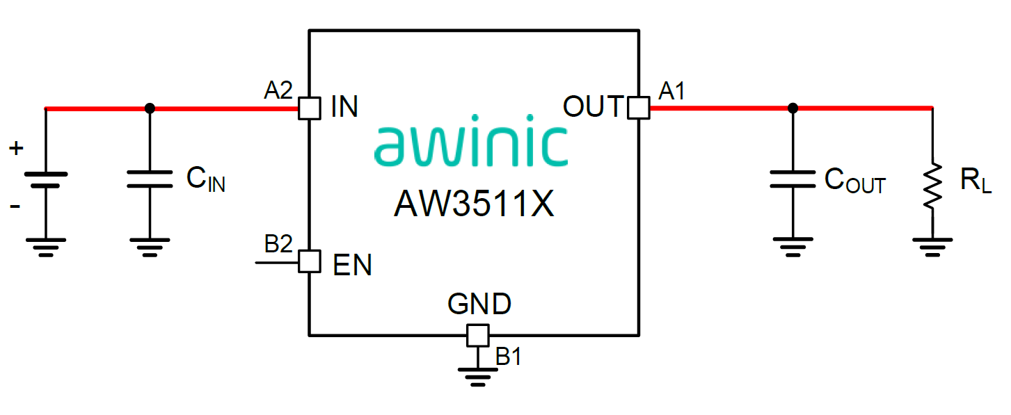
•Integrated P-channel MOSFET load switch
•Input voltage: 1V to 5.5V
•2A maximum continuous switch current
•Switch on-resistance(typ.):
Rdson=52mΩ at VIN=5.5V
Rdson=57mΩ at VIN=4.2V
Rdson=64mΩ at VIN=3.3V
Rdson=76mΩ at VIN=2.5V
Rdson=100mΩ at VIN=1.8V
Rdson=164mΩ at VIN=1.2V
Rdson=230mΩ at VIN=1V
•Controlled slew rate to limit inrush currents
•Ultra low shutdown current
•Internal EN pull-down/up resistor
•Quick Output Discharge(QOD) for AW35111/ AW35113
•Full time Reverse Current Protection (RCP) for AW35112/AW35112B/AW35113
•FCDFN 0.8mm*0.8mm*0.55mm-4L package
FOWLP 0.8mm*0.8mm*0.5mm-4B package
The AW3511X family load switch integrates a 64mΩ (typ.) P-channel MOSFET, which can operate over a wide input range of 1V to 5.5V. The AW3511X features output slew rate control, limiting inrush currents during turn-on to protect downstream devices.
In addition, AW35111/ AW35113 have QOD function which can prevent the output from floating when the switch is disabled.
There is a Reverse Current Protection(RCP) function for AW35112/AW35112B/AW35113 when VOUT is 33mV(typ.) greater than VIN, which can prevent the current to flowing through the P-FET in the body diode. There is no output discharge resistor for AW35112 and AW35112B.